Low-Power AI Semiconductors for High-Performance Neural Networks
Professor Jong-Ho Lee
- Importance of low-power AI semiconductor devices and circuits for on-device AI
- Creative use of vertically stacked non-volatile memory for high-density/low-power AI
- Efficient integration of AI semiconductors and sensors: Artificial olfactory system
Professor Jong-Ho Lee, from the Department of Electrical and Computer Engineering, leads the Semiconductor Materials and Devices Lab (SMDL). This lab conducts research on various non-volatile memory-based devices, their integration process technology, various architectures, and low-power circuit blocks for low-power and highly integrated AI systems. In addition, as an example of applying these AI technologies, we are developing innovative technologies for low-cost integration of gas sensor arrays, synapses, and neurons on the same substrate.
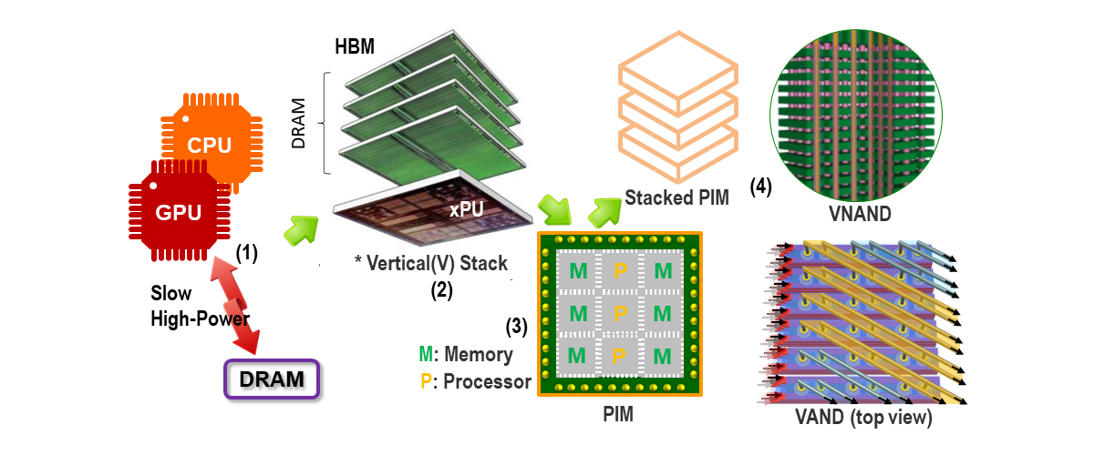
The biggest topic of CES 2024 was by far AI, and what received the most attention was on-device AI, where AI permeates all devices, and AI semiconductors for this. The key to on-device AI is reducing power consumption while maintaining high-accuracy, which can be achieved through algorithmic advancements and low-power hardware and software development. Professor Geoffrey Hinton, who is considered the founder of deep learning, also said at the 'Conversation between the President and AI Scholars' held at the University of Toronto, Canada in September 2022, “The AI revolution will definitely occur once more. The coming revolution is likely to be achieved through hardware innovation,” he said. Current AI technologies mainly rely on stage (1) technology in Fig. 1, and the resulting power consumption in data centers is reaching a serious level1. The issue is latency and power consumption due to data communication between processors and DRAM. A solution to alleviate this issue is HBM (High Bandwidth Memory), shown in stage (2) of Fig. 1, which has recently begun commercialization.
Our lab is developing core technologies that lower-power consumption by more than 10 times compared to current technologies while maintaining high performance. We are developing technologies related to stages (3) and (4) in Fig. 1. In our lab, flash memory devices, ferroelectric tunnel junction (FTJ), and thin film transistors (TFTs) are being researched as device technologies for synapses, and device/circuit technologies to mimic neuron functions are being developed2-5. These synaptic devices are manufactured, various device characteristics are measured and analyzed. The impact of errors occurring in weight transfer on inference accuracy is analyzed. Low-frequency noise is analyzed in various synaptic devices, and how this noise affects inference accuracy is studied. Furthermore, research is being conducted to utilize these noises in AI learning such as reinforcement learning. In addition, low-power peripheral circuits and memory-based low-power circuits are developed, and weighted sums are performed in analog form, greatly reducing power consumption in neural networks. We are also conducting research on various learning methods (on-chip and off-chip learning, hybrid learning) and encoding of signals used in neural networks. In particular, Professor Lee's lab is focusing on research on neural networks using the three-dimensional stacked vertical NAND (VNAND) and vertical AND (VAND) architectures, which are advantageous for achieving high-integration and low-power6,7. Currently, more than 200 floors of VNAND are being mass-produced, and it is scheduled to be mass-produced at more than 300 floors in 2024-258. Therefore, in the near future, cells of more than 1T (tera) bits will be stacked monolithically on a single chip, and this can be said to be the most suitable for implementing synapses with high-density than any other technology. Various AI architectures can be implemented by simply changing the wiring in the currently mass-produced VNAND flash memory7,9. By developing various core technologies utilizing these technologies, it is expected that high-density, low-power, high-accuracy AI networks based on semiconductor memory will be put to practical use in various applications.
Low-power AI semiconductor technology has a variety of applications, including on-device AI. For example, low-power AI technology can be efficiently integrated with a gas sensor array on the same chip. Professor Lee's lab has FET-type gas sensor technology that can detect gas at high speed while consuming the lowest power in the world10. A fast and reliable artificial olfactory system was developed through the efficient fusion of these FET-type sensors and a spiking neural network11. Additionally, a new gas identification method using a gas sensor-amplifier merged array and in-memory computing-based preprocessing was developed12. In this way, this professor's lab is leading the world in this field. In the future, the combination of various sensors and AI will create a variety of useful applications.
*http://wccftech.com/amd-r9-390x-8-gb-hbm/
References
- 1 https://www.sedaily.com/NewsView/2D49DYKEO6
- 2 J.-H. Bae et al., IEEE EDL, 40 (4), 624-627, 2019
- 3 W. Shin et al., AIS, 5 (6), 2200377, 2023
- 4 K.-H. Lee et al., AIS, 6 (1), 2300490, 2024
- 5 D. Kwon et al., Science Advances, 9 (29), eadg9123, 2023
- 6 J. Kim et al., IEDM, 23-4, 2023
- 7 S.-T. Lee et al., Frontiers in Neuroscience 14, 571292, 2020
- 8 https://www.mk.co.kr/news/business/10852012
- 9 S.-T. Lee et al., IEDM, 38.4, 2019
- 10 G. Jung et al., Sensors and Actuators B: Chemical 334, 129642, 2021
- 11 D. Kwon et al., Sensors and Actuators B: Chemical 345, 130419, 2021
- 12 G. Jung et al., IEDM 33-5, 2023