Materials Born and Designed to Be Neuromorphic
Professor Min Hyuk Park
- Innovative Materials Engineered to Emulate Neurological Systems
- Pioneering artificial superlattices with unexpected properties
- Harnessing Interfaces as Cornerstones in Electronic Device Fabrication
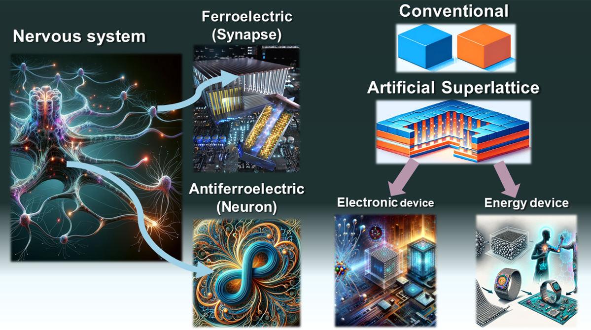
Much like individuals with unique genetic compositions, materials possess inherent traits that significantly influence their suitability for specific applications. By harnessing materials with tailored intrinsic properties, researchers aim to unlock fundamental advantages over conventional random materials. This principle remains valid in the semiconductor realm, particularly within the burgeoning field of neuromorphic computing, which promises highly energy-efficient computational capabilities1-4. Materials are now being engineered to replicate the intricate functions of synapses and neurons, offering promising avenues for neuromorphic computing. This innovative approach involves the creation of artificial superlattices with properties that diverge from those of their constituent materials, effectively leveraging interfaces as novel building blocks for electronic devices.
At the Nano Electronic & Energy Materials Laboratory, led by Prof. Min Hyuk Park, pioneering research is underway to develop advanced materials capable of emulating the biological characteristics of neurons and synapses1-5. Focus is placed on materials like ferroelectric and antiferroelectric substances, which exhibit distinct properties conducive to neuromorphic functionalities. Ferroelectrics, characterized by their ability to polarize without external electric fields, can modulate resistance, simulating synaptic behaviors. Conversely, antiferroelectrics can mimic neuronal activities by generating electrical spikes under specific conditions6-7. These materials show promise in constructing monolithic spiking neural networks, with the research team showcasing world-class expertise in achieving exceptional ferroelectric and antiferroelectric properties in ultra-thin films.
Furthermore, the research group is pioneering the creation of artificial nanostructures to unlock novel material properties or enhance existing ones. For instance, stacking hafnium oxide and zirconium oxide layers in nanometer thicknesses can induce ferroelectric or antiferroelectric properties, exemplifying the potential of combining materials with disparate lattice constants yet similar crystal structures8. By leveraging atomic layer deposition, a technique compatible with complementary-metal-oxide-semiconductor (CMOS) processes, the research group has achieved this feat with simple binary oxides, which holds immense industrial significance in advancing Si-based CMOS processes.
As exploration delves into ultra-thin films at the nanometer scale, attention is directed towards the interfaces between different materials. These interfaces exhibit unique characteristics, influencing phenomena such as the formation of 2D electron gas or permanent dipoles. Leveraging these interface properties, the research team aims to create new artificial materials and electronic devices, with a focus on enhancing ferroelectricity through interface manipulation.
Given the pivotal role of materials in advancing semiconductor technology, the ongoing development of advanced electronic materials in the Nano Electronic & Energy Materials Laboratory holds immense promise for the future of the industry. It is anticipated that these novel materials will contribute significantly in overcoming current and future challenges, akin to historical breakthroughs, propelling the semiconductor industry towards new heights.
References
- 1 J. Y. Park, D. H. Choi, D. H. Lee, J. S. Heo, M. H. Park et al., Adv. Mater. 35, 2204904 (2023).
- 2 T. Mikolajick and S. Slesazeck et al., Adv. Mater. 35, 2206042 (2023).
- 3 D. H. Lee, Y. Lee, and M. H. Park et al., Adv. Funct. Mater. 2303956 (2023).
- 4 U. Schroeder,+ M. H. Park,+ T. Mikolajick, C. S. Hwang, Nat. Rev. Mater. 7, 653 (2022).
- 5 M. H. Park and C. S. Hwang et al., Adv. Mater. 27, 1811 (2015).
- 6 M. H. Park and C. S. Hwang et al., Rep. Prog. Phys. 82, 124502 (2018).
- 7 M. H. Park and C. S. Hwang et al., Nano Energy 12, 131 (2015).
- 8 M. H. Park and C. S. Hwang et al., Appl. Phys. Rev. 6, 041403 (2019).