Ultimately Scaled 2D Semiconductor Electronics for Beyond-CMOS & AI Technology
Professor Chul-Ho Lee
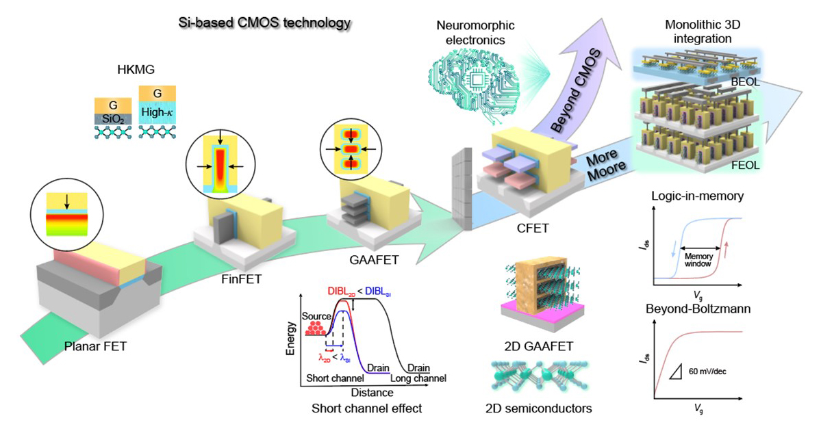
- Overcoming the device scaling limit faced by CMOS technology
- Developing ultralow-power devices and neuromorphic electronics for non-von Neumann computing
- Developing monolithic 3D integration technology for multifunctional hyper-integrated systems
Professor Chul-Ho Lee, from the Department of Electrical and Computer Engineering, leads the Laboratory of Emerging Electronics and optoElectronics (Lab. EEE). This research group is dedicated to advancing Beyond-CMOS and AI technologies through the exploration of atomically thin 2D semiconductor electronics. Their efforts are grounded in a deep understanding of device physics for extremely scaled nanodevices and involve extensive engineering in both new materials and semiconductor processing.
As traditional CMOS technology faces scaling limitations, there is a burgeoning interest in atomically thin 2D semiconductors as next-generation channel materials. These emerging semiconductors boast promising electrical characteristics even at atomic thickness levels, offering remarkable electrical control and high resistance to the short channel effect. Nonetheless, achieving device performance comparable to Si-based CMOS remains challenging. Consequently, the Lab. EEE actively explores various device aspects such as contact engineering, doping techniques, and gate stack optimization to overcome these scaling limits and advance device scaling1-3. The overarching goal is to pioneer innovative strategies for enhancing the performance and reliability of emerging 2D semiconductor electronics.
In tandem with addressing scaling issues, developing ultra-low-power devices and hardware has become imperative due to escalating power consumption and heat dissipation concerns. Leveraging the unique properties of 2D semiconductors, the Lab. EEE endeavors to explore novel devices with significantly lower power consumption than conventional MOSFETs, operating on distinct principles4-5. Among these are novel steep-slope transistors and tunneling field-effect transistors capable of surpassing the fundamental Boltzmann switching limit.
Moreover, overcoming the limitations of traditional von Neumann computing architectures entails delving into novel computing paradigms like in-memory and neuromorphic computing. It is crucial to develop tailored devices and hardware components for such novel computing. In pursuit of this, the Lab. LEE has been at the forefront of developing 2D-semiconductor-based memristors and ferroelectric devices with innovative architectures. Integrating these components into neuromorphic systems offers substantial benefits, including ultra-low power consumption, precise tuning, and multi-signal processing within highly-integrated neural networks. Experimental implementations have demonstrated significant improvements in accuracy, speed, and energy efficiency in recognizing unstructured data through heterosynaptic neuromodulation of artificial synapses employing 2D semiconductors6-8.
Simultaneously, the unique van der Waals layered structures of 2D semiconductors, featuring no physical bonding in the out-of-plane direction, facilitate heterogeneous integration with minimal materials and processing constraints. This enables seamless integration of diverse 2D semiconductor-based electronic and photonic devices, sensors, and memories, propelling the development of multifunctional 3D-integrated electronic systems for future AI and IoT technologies9.
Research endeavors also tackle the challenge of achieving monolithic 3D integration compatible with traditional Si-based CMOS systems. Focus is on low-temperature, high-quality thin film growth of 2D semiconductors and subsequent device fabrication processing with atomic-level controllability10-11. These efforts aim to enable monolithic 3D integration of various functional devices based on 2D semiconductors at back-end-of-line (BEOL)-compatible low temperatures below 400℃, paving the way for future advancements in hyper-integrated electronic systems.
In summary, Lab. EEE's research interest in emerging 2D semiconductor electronics revolves around exploring novel materials, device architectures, and fabrication techniques to surpass current limitations and unlock new capabilities. Their ultimate goal is to make substantial contributions to advancing 2D semiconductor electronics for beyond-CMOS and AI technology, driving innovation and shaping the future of electronic devices and systems.
References
- 1 D. Lee et al., Nature Electron. 4, 664 (2021).
- 2 Y. S. Kim et al., Science Adv. 7, eabd7921 (2021).
- 3 S. Yang et al., Nano Lett. 20, 2443 (2020).
- 4 J. Shin & S. Yang et al., Nat. Commun. 11, 1412 (2020).
- 5 Y. H. Kim et al., Adv. Mater. 10.1002/adma.202314274 (2024).
- 6 W. Huh et al., Adv. Mater. 35, 2211525 (2023).
- 7 W. Huh et al., Adv. Mater. 32, 2002092 (2020).
- 8 W. Huh et al., Adv. Mater. 30, 1801447 (2018).
- 9 S. M. Yang & J. H. Shim et al., Adv. Mat. 34, 2108203 (2022).
- 10 S. Y. Joung et al., ACS Nano 18, 1958 (2024).
- 11 H. S. Kang et al., NPG Asia Mater. 14:90 (2022).