Innovative Synthesis and 3D Integration of 2D Materials for Enhanced AI Computing
Professor Gwan-Hyoung Lee
- Pioneering the synthesis of sing crystal 2D semiconductors through hypotaxy
- Fabricating high-performance nanodevices based on 2D materials
- Advancing monolithic 3D integration techniques for AI computing
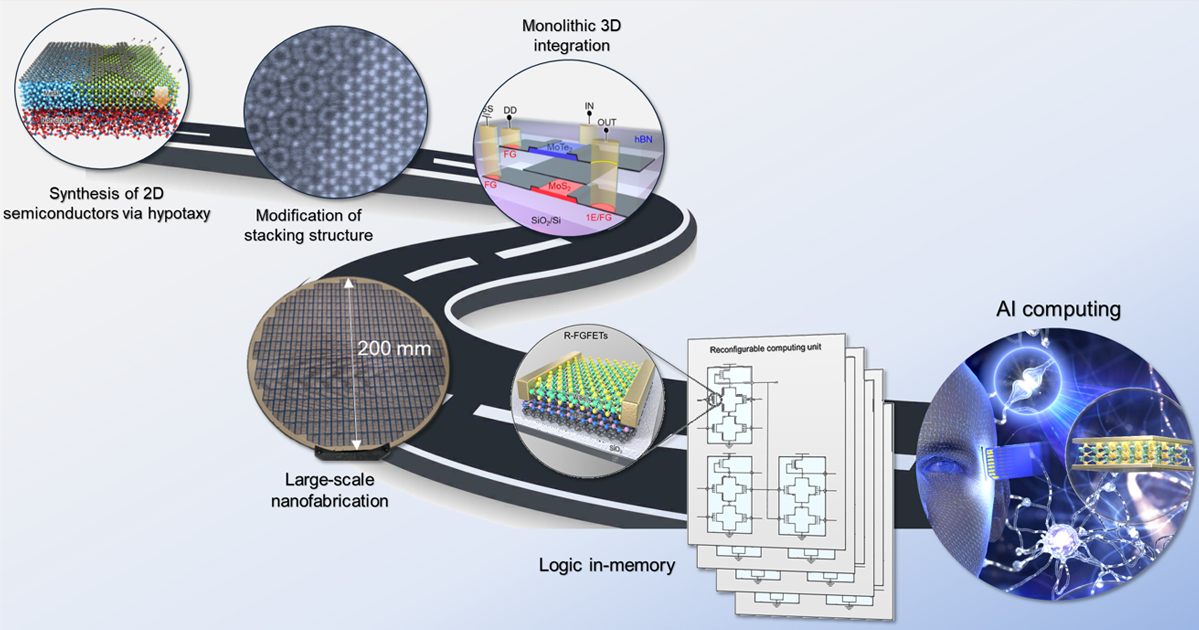
The field of artificial intelligence (AI) computing is witnessing a transformative phase with the advent of advanced semiconductor technologies. A pivotal role in this transformation is played by the research conducted by Professor Gwan-Hyoung Lee's team at Seoul National University. Their groundbreaking work, centered around the monolithic 3D integration of 2D material-based devices, heralds a new era in AI computing capabilities1. The team's research, detailed on their website (http://gwangroup.snu.ac.kr), focuses on the synthesis of 2D materials, the fabrication of high-performance nano-devices using these materials, and their eventual integration into monolithic 3D structures for semiconductor applications in AI computing2.
The cornerstone of Professor Lee's research is the innovative synthesis of 2D materials through a novel technique known as hypotaxy3-4. This pioneering method enables the creation of wafer-scale single crystal 2D semiconductors, such as MoS2, MoSe2, WS2, and WSe2, through graphene nanopores that are pivotal for 3D stacking capabilities. The hypotaxial growth technique enables the growth of 2D semiconductors on various substrates, including those that are amorphous or have lattice mismatches. This method facilitates the precise control of 2D semiconductor thickness and promotes the growth of high-quality monolayer MoS2 with excellent thermal conductivity and carrier mobility. The hypotaxy process not only marks a significant breakthrough in the synthesis of 2D materials but also lays the foundation for the next generation of semiconductor devices. By leveraging this technique, the research team has successfully developed high-performance memory units and transistors with exceptional charge mobility. These advancements are crucial for the miniaturization and enhancement of semiconductor devices, making them highly suitable for AI applications.
The team recently developed reconfigurable floating-gate field-effect transistors (R-FGFETs) based on van der Waals heterostructures for in-memory computing, offering a compact, energy-efficient solution with minimal overhead5. These devices achieve multi-functional operations by modulating charge trapping in a graphene floating gate, enabling four distinct electrical states. The integration of R-FGFETs into a computing unit allows for the implementation of programmable logic and arithmetic operations. The work addresses voltage mismatch issues between input and output, further enhancing the efficiency of logic gate connections. This advancement paves the way for highly integrated, area-efficient reconfigurable processors for advanced computing applications.
Furthermore, the team's expertise extends to the monolithic 3D integration of these devices, a process that involves the vertical stacking and interconnection of multiple layers of 2D material-based devices6-8. This integration technique is instrumental in achieving high-density, high-performance computing systems. The ability to stack devices monolithically offers several advantages over traditional methods, including reduced interconnect lengths, improved energy efficiency, and enhanced computational performance9-11. These attributes are essential for meeting the demanding requirements of AI computing, where speed, accuracy, and efficiency are paramount.
The implications of Professor Lee's research are far-reaching. By pushing the boundaries of what is possible with 2D materials and their integration into semiconductor devices, the team is contributing to the development of AI computing technologies that are faster, more efficient, and more capable than ever before. Their work not only represents a significant advancement in the field of materials science and engineering but also underscores the potential of 2D materials in revolutionizing the semiconductor industry.
Professor Lee said, "Our team is at the forefront of enabling technologies for AI computing. Through our innovative synthesis of 2D materials, fabrication of high-performance nano-devices, and pioneering efforts in monolithic 3D integration, we are setting new standards for the semiconductor industry." As the demand for advanced AI computing continues to grow, the contributions of Professor Lee and his team will undoubtedly play a crucial role in shaping the future of this field.
References
- 1 G. Lee et al., Artificial Neuron and Synapse Devices Based on 2D Materials, Small, 2021, 17, 2100640.
- 2 Xu Cui et al., Multi-Terminal Transport Measurements of MoS2 Using van der Waals Heterostructure Device Platform, Nature Nanotechnology, 2015, 10, 534-540.
- 3 D. Moon et al., Hypotaxy of Wafer-scale Single Crystal Transition Metal Dichalcogenides, under review 2024.
- 4 Y. Jung et al., Nucleation and Growth of Monolayer MoS2 at Multi-steps of MoO2 Crystals by Sulfurization, ACS Nano, 2023, 17, 8, 7865-7871.
- 5 J.-C. Shin et al., Reconfigurable Two-dimensional Floating Gate Field-effect Transistors for Highly Integrated In-memory Computing, under review 2024.
- 6 J.-C. Shin et al., Electrically Confined Electroluminescence of Neutral Excitons in WSe2 Light-emitting Transistors, Advanced Materials, Just accepted 2023.
- 7 J. Kwon et al., 200-mm Wafer Scale Integration of High Performance Polycrystalline MoS2 Thin Film Transistors, Nature Electronics, Just accepted 2023.
- 8 J. Son et al., Atomically-precise Graphene Etch Stops for 3D Integrated Systems from 2D Material Heterostructures, Nature Communications, 2018, 9, 3988.
- 9 Y. Zhang et al., Atom-by-atom Imaging of Moiré Transformations in 2D Transition Metal Dichalcogenides, Science Advances, Just accepted 2024.
- 10 J.-H. Baek et al., Thermally Induced Atomic Reconstruction into Fully Commensurate Structures of Transition Metal Dichalcogenide Layers, Nature Materials, 2023, 22, 1463-1469.
- 11 H. Kim et al., In-plane Anisotropy of Graphene by Strong Interlayer Interaction with van der Waals Epitaxially-grown MoO3, Science Advances, 2023, 9, eadg6696.