From left, Professor In-Suk Choi, Professor Jyh-Ming Lien, and Researcher Yu-Ki Lee
A joint research team consisted of Professor In-Suk Choi, Professor Young-Chang Joo and Professor Myoung-Gyu Lee of the Department of Materials Science and Engineering, Professor Changsoon Kim of the Graduate School of Convergence Science and Technology, Professor Jyh-Ming Lien of George Mason University (including other Seoul National University College of Engineering joint researchers) has developed a technology, utilizing Machine Learning Algorithms that wrap flexible devices on an arbitrary 3D-curved surface without fracture or severe deformation.
Following the recent active research on the development of flexible electronic devices, limitations have been found that commercialized flexible devices cannot be transformed into arbitrary complex forms due to material constraints.
For instance, a flat flexible TV can bend in one direction, but cannot be transformed into a complete sphere. This is because materials used in commercialized devices such as silicon wafers and glass panels are 2D-sheets that are brittle and vulnerable even to small stresses.
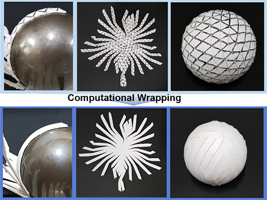
In response, a joint research team succeeded in stably attaching flat-shaped materials such as steel plates and silicon wafers to arbitrary 3D-curved surfaces without damaging them by using optimized planar figures created by Machine Learning.
The researchers adopted an algorithm that approximates arbitrary complex 3D-curved surfaces to a small grid (mesh) and then transfers it in 2D surfaces without overlap. In the process, a Machine Learning technique, called Genetic Algorithm, was used to create a non-overlapped and optimized planar figure even in 3D-curved surfaces comprised of more than hundreds of meshes.
The researchers suggested a methodology for cutting the electrode materials with a generated planar figure and fabricate corresponding flexible devices that could be wrapped around the original 3D-curved surface. By minimizing the effective area of the planar figures obtained through the algorithm, it also minimizes the waste of electrode materials during the cutting process.
In addition, due to the fact that the 3D-curved surfaces consist of more than hundreds of grids, researchers can generate the original smooth 3D-curved surfaces by ignoring crease lines between adjacent grids, bending and pressing the planar figure on the 3D-curved surfaces, not the approximated folded 3D shapes with meshes.
The researchers also discovered that fragile materials such as silicon wafers can be attached stably to various shapes of 3D-curved surfaces without fracture or damage because the optimized planar figure is strain-controlled. Furthermore, the light-emitting devices that contain brittle materials such as ITO (Indium Tin Oxide) can wrap a complex 3D-curved surface and operate well without failure.
SNU Professor In-Suk Choi explained that "This study is significant in that it provides a methodology, using only the Machine Learning algorithm, that we can stably wrap any 3D-curved shapes with non-stretchable materials without any cracks or gaps," and added, "As various devices currently in use can be produced into diverse shapes without new materials or fabrication processes, it will be used in various fields such as wearable/skin-attachable devices, architectural design, and interior/exterior vehicle designs in the future."
The research findings were published online on the <
Science Advances> on April 10th, 2020.
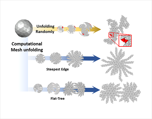
It is difficult to transfer a 3D figure that is approximated by more than hundreds of grids to a 2D figure without overlap. The researchers used a Machine Learning Algorithm that can control the final shape of the planar figure without overlap after unfolding.
The 3D shape can be approximated by bending rather than folding with enough meshes, suggesting a methodology for attaching the materials to a 3D shape without any gaps and damages.
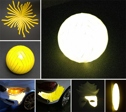
The researchers demonstrated that highly brittle materials such as ITO (Indium Tin Oxide) can wrap arbitrary 3D shapes without failure or damage.
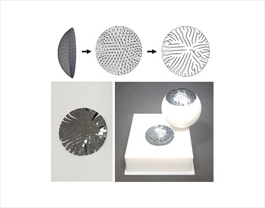
Using the technology presented by the researchers, silicon wafers used by various electronic devices can also be transformed into arbitrary 3D shapes by controlling only the geometry. It has been discovered that the silicon wafers were not fractured even after attaching them to curved surfaces.
For further information, please contact Prof. In-Suk Choi.
