Applicable to next-generation optoelectronic circuits
Light emitting field effect transistor capable of multi-operation mode
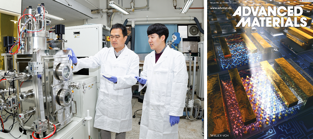
From left, Professor Gwan-Hyoung Lee, Doctor Junyoung Kwon, and the Research Paper Cover Image
A team led by Professor Gwan-Hyoung Lee of the SNU Department of Materials Science and Engineering has developed light-emitting field-effect transistors (LEFETs) based on van der Waals heterostructure that enables multioperation-modes modulated by gating. Not only can it be used as a triad device due to its multioperation-modes, but it also shows the world's highest efficiency in the 2D material-based light emitting devices that can be used in various fields, such as next-generation optoelectronic circuits. This work was published online in Advanced Materials, a world-renowned scientific journal, in September 2020 and was selected to be the front cover image of the journal.
2D semiconductors such as transitional metal dichalcogenides (TMDs) have a great potential for next generation optoelectronic applications due to the large binding energy of exciton (particles with electrons and holes combined) and strong light matter interaction. Therefore, they have been used in the optoelectronic devices with exceptional functions of chiral light emitters and transport of exciton complexes that have not been realized in bulk materials. These researches have demonstrated various functionality of 2D-material-based optoelectronic devices, but it was still challenging to achieve high efficiency of light emission.
The efficiency at room temperature was especially low due to the high Schottky barrier for injection of electrons and holes into the TMDs.
The efficiency at room temperature was especially low due to the high Schottky barrier for injection of electrons and holes into the TMDs.
Professor Gwan-Hyoung Lee and Professor Chul-Ho Lee of KU-KIST Graduate School of Converging Science & Technology developed highly efficient light-emitting field-effect transistors (LEFETs) by using two-dimensional materials: graphene as electrodes and mono-layer WSe2 as a channel that has ambipolar characteristics to transport both electrons and holes.
In the metal electrodes deposited on the WSe2, only one type of electron or hole charge carriers can be injected into the WSe2 channel due to the Fermi level pinning effect. To solve the problem, Professor Lee's team used graphene as the electrode for van der Waals contact without Fermi level pinning. Because the work function of graphene can be modulated by the electric field, electrons and holes can be efficiently injected into WSe2 by controlling the work function of graphene.
By optimizing the numbers of injected electrons and holes with tunable graphene electrodes, Professor Lee's team achieved strong electroluminescence from LEFETs with a high external quantum efficiency of ~ 6 % at room temperature. In addition, three distinct operation modes of the WSe2 LEFETs were demonstrated by controlling the polarity of WSe2 and the contact barrier of the graphene-WSe2 junction with gate voltage, which enables to use the LEFETs as unit devices for multi-functional optoelectronics.
Professor Gwan-Hyoung Lee said, "We accomplished realization of all-2D-material-based optoelectronic devices and improvement of light-emitting efficiency through 5 years of research. It is expected that the LEFETs, which mainly utilizes the work function modulation of graphene, will be used in next-generation optoelectronic circuits.”
The research findings were published online on September 11 in <Advanced Materials>.
For further information, please contact Prof. Gwan-Hyoung Lee.
